It is 2013, and a back-of-envelope calculation inside Google produces an uncomfortable number: if every user ran voice search for three minutes a day, running that workload through the deep neural networks then in use would require doubling the number of Google datacenters. General-purpose processors were about to become too expensive to think with. Two years later, Google has already deployed a custom chip built to make one calculation, and one calculation only, absurdly cheap.
Where We Were
By the early 2010s the ingredients of the deep-learning boom were in place but running on borrowed hardware. Deep belief networks had shown that deep nets could be pretrained layer by layer (engine room, Chapter 1), CUDA had turned graphics chips into general math engines from 2007 (engine room, Chapter 2), and AlexNet’s 2012 ImageNet win had proven that GPU-trained convolutional networks beat every hand-engineered alternative. All of this ran on processors designed for something else — CPUs built for branchy, latency-sensitive code, GPUs built for rendering triangles and only recently repurposed for matrix multiplication.
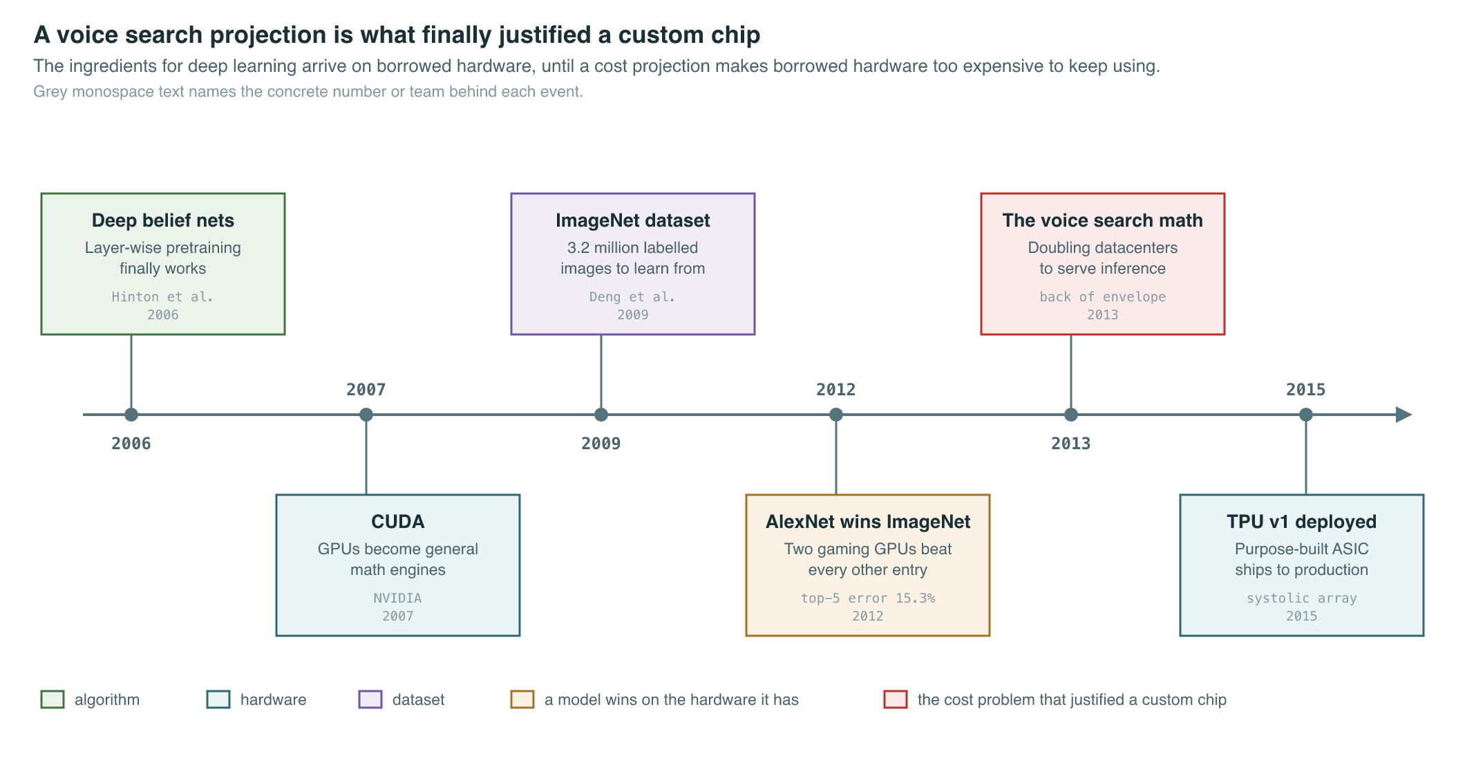
The problem Google faced was not training — it was serving. A model trained once runs inference billions of times a day, and by 2013 neural networks were quietly taking over Search ranking, Photos tagging, Translate, and speech recognition. GPUs of that generation were built to maximize floating-point throughput for graphics and scientific workloads; they carried hardware for tasks — texture units, double-precision paths, complex scheduling for irregular kernels — that a production inference workload never touches. Running that workload at Google’s scale on general-purpose silicon meant paying, in power and in datacenter floor space, for capability nobody was using. This is a compute-economics problem before it is an engineering one: a datacenter’s power and cooling budget is fixed by its building, not by demand, so every watt a chip spends on a capability the workload doesn’t use is a watt unavailable for more inference. The company’s response was to stop asking general-purpose chips to do a specific job well and instead build a chip that could do nothing else.
The Breakthrough
Google’s answer was the Tensor Processing Unit, an application-specific integrated circuit whose entire purpose is the one operation that dominates neural-network inference: multiply a matrix of weights by a matrix of activations, over and over, at low numerical precision. The team designed, verified, built, and deployed the first TPU into production datacenters in about fifteen months — deliberately skipping the years of iteration a general-purpose processor demands, because the target was narrow enough to hit on the first pass. The chip went into production in 2015; the architecture and its production results were made public two years later in “In-Datacenter Performance Analysis of a Tensor Processing Unit” (Jouppi et al., 2017).
The chip’s core is a systolic array — a grid of arithmetic units, 256 by 256 of them, wired only to their immediate neighbors. “Systolic” describes how data moves through it: in coordinated waves, the way blood is pumped through a heart, rather than being fetched from and written back to memory at every step. Weights are loaded into the grid once and held there; activations stream in from one edge, partial products pass from cell to cell, and finished output values emerge from the far edge, all without any intermediate result touching memory. That single design choice — reuse a loaded weight across many multiplications instead of re-reading it — is what makes the chip’s math section below work, and it is the reason a TPU can dedicate almost its entire die to arithmetic rather than to the caches and control logic a general-purpose CPU or GPU needs to keep memory-bound execution fed.
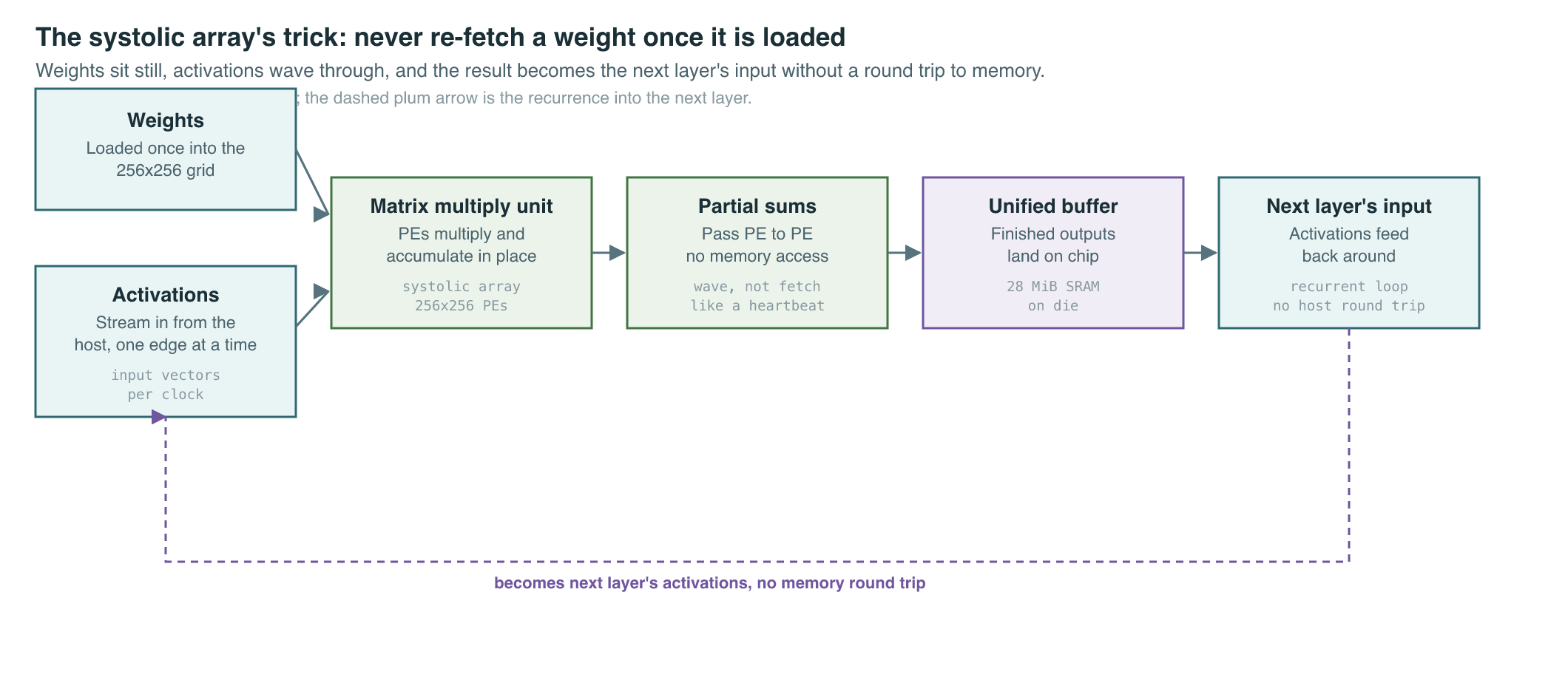
The first-generation TPU was narrow by design: an 8-bit integer matrix unit with 65,536 multiply-accumulate cells, clocked at 700 MHz, drawing about 40 watts on a 28-nanometer process — roughly half the die area of a contemporary CPU or GPU. Google’s own comparison against a contemporaneous Haswell CPU and an Nvidia K80 GPU, running the same production inference workloads (multilayer perceptrons, convolutional nets, and LSTMs that by then accounted for roughly 95 percent of the company’s datacenter inference demand), found the TPU 15 to 30 times faster and 30 to 80 times better in operations per watt. It was not a faster general-purpose chip; it was a chip that had given up generality entirely to win at one thing.
The Mathematics
The systolic array’s appeal is not just that it is fast — it is that its speed follows directly from geometry, with no cache hierarchy or instruction dispatch in the loop. A grid of multiply-accumulate cells, each producing one multiply and one add (2 floating-point operations) per clock tick, has a peak throughput fixed entirely by its size and its clock speed:
The second reason the design works is what it does to memory traffic. Because a loaded weight stays resident in its cell rather than being re-fetched, the chip’s arithmetic intensity — operations performed per byte moved from memory — is not fixed by the hardware at all; it grows with how long you keep streaming activations through the same weights:
| Symbol | Meaning |
|---|---|
| peak operations per second of the systolic array | |
| side length of the square array of multiply-accumulate cells | |
| clock frequency | |
| arithmetic intensity, operations performed per byte of memory traffic | |
| number of activation vectors streamed while weights stay resident | |
| bytes used to store one weight element |
What It Enabled
The first TPU proved the bet: a narrow, purpose-built chip could beat general-purpose silicon on the workload that mattered most to its owner, by a wide enough margin to justify designing and fabricating custom ASICs at all. Google kept iterating on the same recipe — bigger systolic arrays, more chips wired into ever-larger pods, and eventually its own optical networking to rewire those pods on the fly.
| Generation | Announced | Peak compute (per chip) | Memory | What changed |
|---|---|---|---|---|
| TPU v1 | 2015 (paper: April 2017) | ~92 TOPS (int8) | 8 GB, no HBM | Inference-only systolic ASIC; proved the concept |
| TPU v2 | May 2017 | ~45 TFLOPS (bf16) | 16 GB HBM | Added bfloat16 floating point — could train, not just serve |
| TPU v3 | May 2018 | ~123 TFLOPS (bf16) | 32 GB HBM | Liquid cooling; roughly 2.7x v2 per chip |
| TPU v4 | May 2021 (paper: April 2023) | 275 TFLOPS (bf16) | 32 GB HBM | Optical circuit switches for reconfigurable pod topology; SparseCores for embeddings; 4,096-chip pods exceeding 1 exaflop |
| TPU v5e | August 2023 | 197 TFLOPS (bf16), 393 TOPS (int8) | 16 GB HBM | Cost-optimized inference and training part of the split line |
| TPU v5p | December 2023 | 459 TFLOPS (bf16) | 95 GB HBM | Scale-optimized training part of the split line, aimed at the largest models |
| TPU v6e, “Trillium” | May 2024 | 918 TFLOPS (bf16), 1,836 TOPS (int8) | doubled HBM vs v5e | MXU widened back to 256x256 — a return to TPU v1’s array size, five generations and roughly 20x TPU v1’s peak int8 throughput later |
TPU v4 is where the “pod” idea matured into a full supercomputer. Google’s own figures put it at 2.1 times the raw performance and 2.7 times the performance-per-watt of TPU v3, at 4.3 to 4.5 times the speed of a contemporary Graphcore IPU Bow, and 1.2 to 1.7 times faster than an Nvidia A100 while drawing less power — the A100 itself is covered as part of the broader accelerator economics of Chapter 20. The optical circuit switches that let Google rewire a 4,096-chip pod’s interconnect topology on demand added under 5 percent to system cost and 3 percent to power draw, in exchange for a network that could be reconfigured around failed links instead of stalling. That scale is what made PaLM possible: a single 540-billion-parameter model trained across 6,144 TPU v4 chips split over two pods, at 46.2 percent of the hardware’s theoretical peak utilization — the model itself belongs to Chapter 10, but the number is a direct readout of what this chapter’s pod architecture bought.
The split after v4 made the specialize-versus-generalize question explicit within Google’s own product line. TPU v5e, announced in August 2023, optimized for cost per inference and per training dollar rather than raw peak performance — Google’s own marketing put it at under half the cost of TPU v4 for comparable work. TPU v5p, announced that December, went the other way: pods of 8,960 chips wired over a higher-bandwidth interconnect, aimed squarely at training the largest models as fast as possible, with Google claiming roughly 2.8 times the training speed of v4. Trillium, the sixth generation unveiled in May 2024, widened the matrix multiply unit back to 256x256 — TPU v1’s original array size, five generations and roughly 20 times TPU v1’s peak int8 throughput later — and Google described it explicitly as the silicon underlying the next generation of Gemini models, closing the loop between this chapter’s hardware and the language-model chapters it feeds.
TPU v1’s real legacy, though, was less the chip than the argument it settled: specialization pays, and other companies pursued the same argument to more extreme conclusions than Google did. Cerebras took the opposite path to avoiding chip-to-chip interconnect losses — instead of networking many small dies together, it fabricated a single processor from an entire silicon wafer. The first Wafer Scale Engine, unveiled in August 2019, packed 1.2 trillion transistors and 400,000 cores onto 46,225 square millimeters of silicon, next to which contemporary GPU dies looked like fragments; the second generation, in April 2021, pushed that to 2.6 trillion transistors and 850,000 cores on the same wafer footprint. Groq specialized differently again: its Tensor Streaming Processor, described in “Think Fast: A Tensor Streaming Processor for Accelerating Deep Learning Workloads” (Abts et al., ISCA 2020), threw out caches, out-of-order execution, and even DRAM in favor of a single deterministic core whose instruction schedule is fixed entirely at compile time and whose working set lives in on-chip SRAM. Groq later re-marketed the same chip as the Language Processing Unit, aimed specifically at the low-latency token-by-token generation that inference serving demands — ground covered from the serving side in Chapter 17.
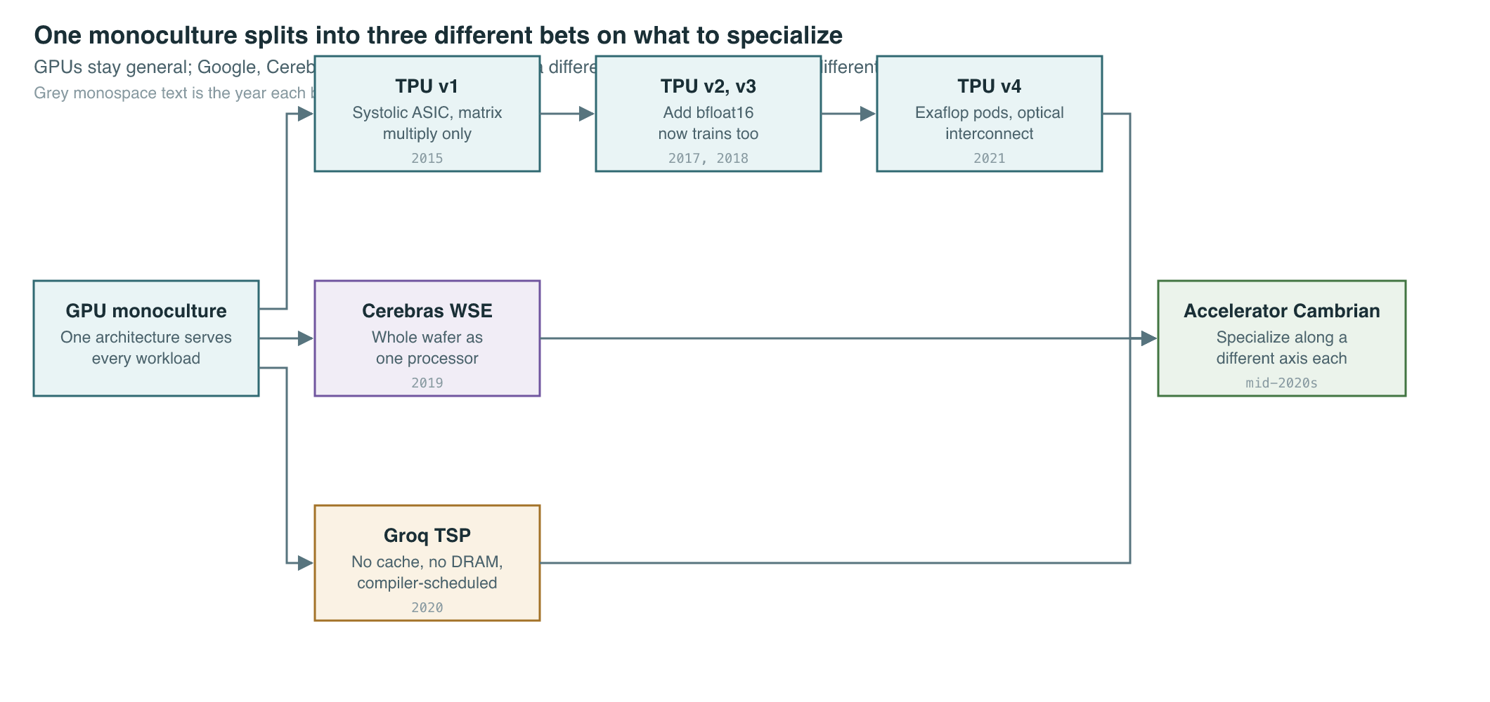
By the early 2020s the industry had split along a specialize-versus-generalize axis, and each point on it made a different bet about what stays fixed.
| Accelerator | Specialization axis | What it trades away | Where the bet paid off |
|---|---|---|---|
| GPU (Nvidia line) | General-purpose parallel compute, huge software ecosystem | Peak efficiency on any single workload | Training and inference across nearly every model architecture, backed by CUDA — Chapter 2 |
| Google TPU | Matrix-multiply-first ASIC, systolic dataflow, custom interconnect | Flexibility outside Google’s own software stack | Google’s internal training and serving fleet, from Search to Gemini |
| Cerebras WSE | Wafer-scale integration, everything on one die | Manufacturing yield and cost per chip | Workloads that hate chip-to-chip communication — very large models, very long sequences |
| Groq LPU | Deterministic, compiler-scheduled, SRAM-only dataflow | Model flexibility and on-chip memory capacity | Latency-critical LLM token generation |
None of these designs displaced the others; they cohabit because “specialize” is not one decision but several — precision, memory hierarchy, interconnect, and software stack can each be narrowed independently, and each accelerator in this chapter narrowed a different subset. The through-line into later chapters is that this specialization race did not stop at the chip: Chapter 13 covers routing computation to specialized sub-networks, and Chapter 20 closes the book’s argument that model architectures and accelerator designs have been shaping each other, not evolving independently, since roughly this point in the timeline.
Key Papers
| Paper | Authors | Year | Link | Why it matters |
|---|---|---|---|---|
| In-Datacenter Performance Analysis of a Tensor Processing Unit | Jouppi et al. | 2017 | arXiv:1704.04760 | First public disclosure of TPU v1’s systolic-array design and its production performance and efficiency numbers against contemporary CPUs and GPUs |
| TPU v4: An Optically Reconfigurable Supercomputer for Machine Learning with Hardware Support for Embeddings | Jouppi et al. | 2023 | arXiv:2304.01433 | Documents the pod-scale architecture — optical circuit switches, SparseCores, 4,096-chip pods — that underwrote large-scale training runs like PaLM |
PM Lens
Papers referenced
- In-Datacenter Performance Analysis of a Tensor Processing Unit Jouppi et al. · 2017 · arXiv:1704.04760
- TPU v4: An Optically Reconfigurable Supercomputer for Machine Learning with Hardware Support for Embeddings Jouppi et al. · 2023 · arXiv:2304.01433